
MEMS - Deep Glass Machining
Masking Materials for Deep Glass Micromachining
(by Dr. Daniel C. S. Bien and Dr. Paul V. Rainey)
Bulk micromachining of glass is widely used for the fabrication of many microfluidic structures, such as fluid flow channels and thin diaphragms for pumps, active valve and dispenser applications. Glass substrates have the advantage of transparency, which allows fluid flow through the channels to be easily detected and monitored. The research focus on the various materials that can be used as a mask during anisotropic etching of glass substrates in concentrated HF 48 %. All the materials that were investigated can be easily deposited and lithographically patterned. Etching test were done on 100 mm diameter, 0.75 mm thick glass wafer (Corning 1737 – Aluminosilicate Glass) with Rms Roughness, Rrms of 1.38 nm and peaks less than 20 nm.
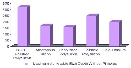
From the results obtained, Microposit 1813 photoresist masking only allows shallow etching (depth < 50 mm). Thick SU-8 photoresist alone is not suitable as masking material due to its poor adhesion to oxide surfaces. The best results were obtained with a combination of polished polysilicon and thick SU-8 photoresist as masking material with etch depths of more than 300 µm achieved. This is 6 times deeper than that obtained using standard photoresist. The polished polysilicon material acts as an interface layer for the SU-8 and also as a secondary protection to the glass substrate. The other masking materials investigated were only suitable for etch depths of less than 200 µm. For etch depth greater than 200 µm, the concentrated HF etchant penetrates the mask and roughens the glass surface. Gold electroplating is particularly effective when used to protect exposed adhesion layers such as titanium, at the edges of patterned features.
In the case of polysilicon, surface spikes in the material cause poor coverage by standard photoresist, resulting in indentations in the masking layer during polysilicon etching. These indentations result in premature penetration of the mask while etching the glass. Polishing of the polysilicon reduces the surface spikes and prevents the indentations; however the thickness of polysilicon covering asperities on the glass surface will be reduced. Slow etching of the polysilicon in HF leads to penetration of the mask at these locations. Penetration of the gold masking material is believed to be due to particles deposited on the wafer in the sputtering chamber. Therefore particle-free processing is of prime importance in the fabrication of effective masking layers.
References
- Bien DCS, Rainey PV, Mitchell SJN and Gamble HS, “Characterisation of masking materials for deep glass micromachining”, Journal of Micromechanics and Microengineering, vol. 13, ppS34-S40, July 2003.
- Bien DCS, Rainey PV, Mitchell SJN and Gamble HS, “Characterization of masking materials for deep glass micromachining”, Proc. Micromechanics Europe Workshop MME 2002, pp103-106, Sinaia Romania, Oct. 2002.
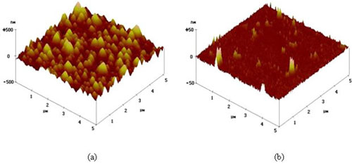 AFM scans showing the roughness of (a) unpolished and; (b) polished polysilicon