
Integrated Circuits and Electronic Devices
The facilities at QAMEC allow the fabrication of complete devices from mask design and fabrication to metalisation
- Charged-Couple Devices (CCD) Technology
- Silicon Carbide Emitter NPN Bipolar Transistors
- Thin Film Transistors (TFT)
Charge Coupled Devices
A 10-mask process has been designed and implemented to fabricate buried n-channel back-illuminated 3-phase CCDs. The mask design incorporates 8x8 and 16x16 arrays based on a 30x30µm pixel size, and employing a single readout register with charge sensing performed by a floating diffusion structure linked to a single source follower transistor. A wide range of test structures has been included in the design to permit measurement of layer resistivities, gate dielectric quality, field threshold voltage, gate length effects, etc. Mask set production has been carried out in the QAMEC facility.
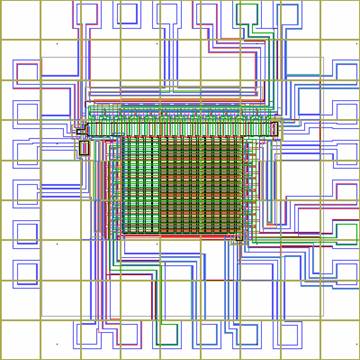
Mask Layout for CCDs Fabrication
Bipolar Transistors
These SEM images show NPN bipolar transistors fabricated as part of a Research Council project which demonstrated the use of silicon carbide (SiC) as the emitter material in a silicon-based heterojunction bipolar transistor (HBT). SiC has a relatively wide bandgap of 2.2eV, and it exhibits high thermal stability, controllable conductivity, and high electron saturated drift velocity. This project avoided the high thermal budgets often associated with SiC deposition by employing Rapid Thermal Processing (RTP) to grow in-situ doped SiC layers using silane (SiH4), propane (C3H8) and phosphine (PH3) gas chemistry. The purpose-built RTP reactor also included the facility to perform in-situ silicon surface cleans using microwave plasma etching. The SiC NPN bipolar transistors fabricated using this technique displayed increased common-emitter current gain compared to standard devices, which was directly attributable to the action of the heterojunction emitter.
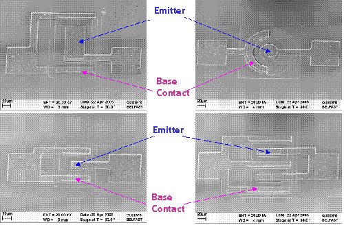
Four base emitter images
Thin Film Transistors
Thin Film Transistors on glass are employed in display technology for pixel switching and for drive cct fabrication. At Queens University Belfast, research in TFT technology ranges from LPCVD polycrystalline silicon/amorphous silicon TFTs to transistors fabricated on single crystal silicon on glass, created using anodic bonding and mechanical thinning technology. Due to temperature restrictions associated with the glass substrate, a low temperature process (<650 °C) has been developed.
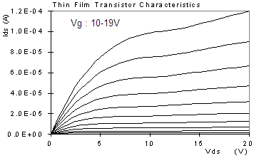
Figure 1(a). Polysilicon TFT Characteristics.
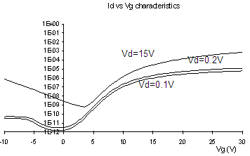
Figure 1(b). Polysilicon TFT Characteristics.
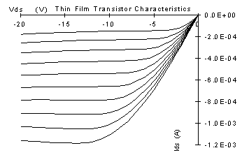
Figure 2(a). Single Crystal Silicon TFT Characteristics.
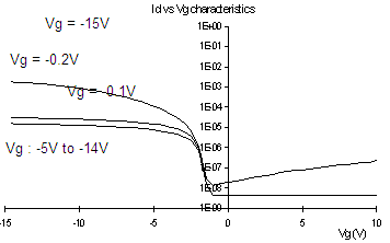
Figure 2(b). Single Crystal Silicon TFT Characteristics.