
Sputtering
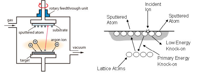
Sputtering, as differentiated from the generic term of PVD which also encompasses evaporation, is the process whereby material is dislodged and ejected from the target through momentum exchange between the target atom and the energetic process gas atom.
Radio frequency (r.f.) or DC are used to generate a plasma, r.f. was developed for the deposition of insulator as the r.f. prevents charging of the target associated with DC. Using these techniques just about any material can be deposited. In contrast chemical vapour deposition (CVD) requires the development of specific volatile precursors.
The uniformity of sputtered layers can be extremely good, as illustrated by its use in the fabrication of giant magneto resistive (GMR) heads. The fabrication of these structures requires the deposition of layers in the order of a few tens of angstroms.
It is this versatility and controllability in conjunction with its superior step coverage when compared to e-beam or thermal evaporation PVD deposition techniques that has made sputter deposition the workhorse of metallisation for IC.
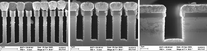
There is a limit to the step coverage possible using a line of sight deposition process such as sputtering as illustrated by the micrographs below.
New sputtering techniques such as long throw or resputtering have been developed to overcome this limitation.
Targets available for sputtering : Tungsten (W), Titanium (Ti), Tantalum (Ta), Copper (Cu), Nickle (Ni), Silicon (Si), Gold (Au), Aluminium (Al)
Recommended reading: Semiconductor Materials and Process Technology Handbook for VLSI and ULSI. Edited Gary E. McGuire Noyes Publication ISBN 0-8155-1150