
CVD Tungsten
Chemical Vapour Deposition is a technique of depositing a wide variety of layers from conductors to epitaxial semiconductors to insulators. All these types of deposition involve the thermally induced reaction of the species carrying molecule on a heated surface. The reaction can take place by a thermal process known as pyrolysis, by a reducing gas, by the substrate or through a combination of these.
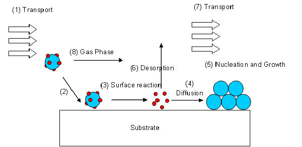
A volatile precursor is transported (1) into the reactor and to the substrate surface, where it adsorbes (2) and reacts (3) to liberate the transporting ligands/reaction by-products, which are subsequently desorbed (6) and transported out of the reactor (7). The metal atoms then diffuse (4) to form stable nucleii, where subsequent growth occurs (5). The surface reactions are determined by the precursor, surface, temperature and other gases, adsorbed onto the substrate surface.
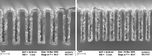
This desired operating regime is known as kinetic or surface reaction controlled deposition. As it is the reaction at the surface of the substrate that determines the deposition rate this process will produce conformal layers over the entire substrate.
The tungsten precusor is tungsten hexafluoride, WF6. WF6 is a quite volatile liquid at room temperature, the vapor is delivered to the reaction chamber through a mass flow controller from the reservoir. WF6 reacts readily with any moisture present to produce tungsten oxides and hydrofluoric acid, HF. It is imperative to avoid moisture in the plumbing: purged high quality stainless steel and metal seals are required.
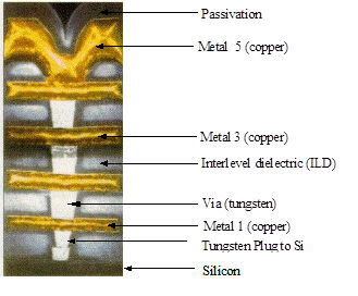
In the semiconductor industry CVD tungsten has found a very particular niche because of its properties and its ability to deposit uniformly over patterned substrates. It’s most common application has been and continues to be the filling of vias between metallisation levels and contacts windows to device silicon.
CVD Tungsten requires a an adhesion or nucleation layer to allow deposition on dielectrics, typically Ti or TiN.
Blanket Tungsten Deposition
The most frequently used chemistries for the deposition of tungsten are SiH4-WF6 and H2-WF6. In these chemistries, silane and hydrogen act as reducing agents for the WF6 precursor. The deposition reactions are summarised below
WF6(g) + 3H2(g) ------------> W(s) + 6HF(g) (1)
2WF6(g) + 3SiH4(g) ------------> 2W(s) + 3SiF4(g) + 6H2(g) (2)
H2-WF6 chemistry is used almost exclusively for blanket deposition of tungsten and the deposition mechanism is well understood. It does, however exhibit very aggresive behaviour against silicon through an initial reaction between the WF6 and the Si. This can result in encroachment and tunnel formation. This is unacceptable as these features can cause junction leakage, compromising device performance and reliability.
SiH4-WF6 chemistry is less violent than H2 reduction when deposition is carried out on silicon and shows none of the signs of substrate encroachment associated with H2 reduction. The quality of the deposited tungsten layer in particular the resistivity is determined by the SiH4-WF6 ratio. Unfortunately, the step coverage of this deposition reaction is not as good as that of H2 reduction and so it is not usually employed for via/plug refilling between metallisation levels. It is, however, still maintained as the initial CVD tungsten deposition when depositing a tungsten contact to silicon. This initial SiH4-WF6 tungsten deposition prevents WF6-H2 attacking the silicon, preventing encroachment problems and tunnel formation. The SiH4-WF6 deposition reaction has not been studied to such a great degree as H2-WF6 chemistry.
Selective deposition
Selective deposition is defined as the preferential deposition of the deposited layer on one material over another. This can be achieved by the reaction between WF6 and silicon. It is this reaction that causes the encroachment problems in H2 chemistry, the presence of SiH4 supresses this step.
2WF6(g) + 3Si(s) ----------> 2W(s) + 3SiF4(g) (3)
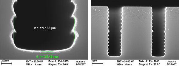
The reaction can only take place as long as silicon is available at the surface and is extremely fast stopping after a certain thickness of tungsten is formed. The tungsten layer acts as a barrier, hence the reaction is self-limiting. Equation (3) only holds for temperatures up to 400°C.
At T > 400°C the reaction is given by (4)
WF6(g) + 3Si(s) ----------> W(s) + 3SiF2(g) (4)
The self-limiting thickness has been reported to vary from 10nm to almost 1.5mm. There is evidence that the reaction between the silicon and the WF6 proceeds at the tungsten surface, the reaction is sustained by the diffusion of silicon through the tungsten layer. The limiting thickness is determined by the silicon surface cleanliness and the base pressure of the deposition system. Hence the discrepancies in the reported self-limiting thickness.
The excellent conformality of the self-limiting layer means it has found a new application as a wear resistant coating on silicon MEMS structures.Tungsten coating adheres well and is hard and conducting, requirements for device performance. Furthermore, since the deposited tungsten infiltrates-under adhered silicon parts and the volume of W deposited is less than the amount of Si consumed, it appears to be possible to release stuck parts that are contacted over small areas such as dimples. The wear resistance of selectively coated W parts has been shown to be significantly improved on microengine test structures.
Thicker selectively deposited layer can be achieved usng either H2-WF6 chemistry or SiH4-WF6 chemistry.
Recommended reading: Chemical Vapour Deposition of Tungsten and Tungsten Silicides for VSLI/ULSI Application by John E. J. Schmitz ISBN 0-8155-1288-2 Noyes publications.