
CVD of Tungsten Silicide
Chemical Vapour Deposition of Tungsten Silicide (WSi2)
Amorphous, silicon rich WSix is deposited using WF6, SiH4 chemistry. A process was established that yielded a W:Si ratio of 1:2.6 established through SIMs analysis.
Silicon rich WSix deposited layer is prefered as it is reported that the incorporation of extra silicon into the layer stabilises the layers during subsequent heat treatment, this is paricularly true for deposition on dielectric substrates. In addition, as the deposited layer is Si rich, no Si is required from the substrate to form WSi2. Hence there is no consumption of the silicon substrate. On annealing this layer converts to a crystalline WSi2 (resistivity 50-60mWcm) and the surplus silicon migrates to the Si/WSi2 boundary as shown in micrographs below.
WSi2 was investigated as a low sheet resistance (200nm r ~ 50mWcm), thermally stable material (no agglomeration up to 1150°C t ~ 200nm) which would be suitable for incorporation into SOI substrates. Tungsten silicides have successfully been incorporated into SOI substrates as a ground planes, buried conduction layers and buried reflector layers.
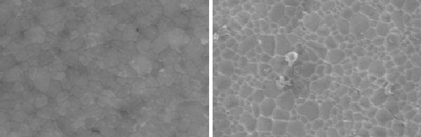
Micrograph above shows grain structure of annealed WSi2 layer and the surface of the silicon substrate after the WSi2 has been removed. The excess silicon that has segregated to the WS/Si interface acn be seen clearly
In the work carried out at QAMEC the most important property of WSi2 has been its ability to withstand high temperatures (T>1000°C) without compromising the layer. This allows high temperature depositions, densification and of particular interest bonding/bond annealing. This has facilitated the integration of buried tungsten silicide layers in novel silicon on insulator (SOI) structures.
For more details see the SOI section >>
Dopant diffusion in WSi2
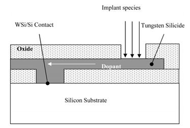
Dopant diffusivity in WSi2 has been evaluated using test structures shown in figure below. The dopant implant window is connected to a substrate contact window by a WSi2 conduit of varying length. The WSi2 contact to the silicon initially forms a Schottky diode. This contact can potentially be modified to become a bipolar diode or an ohmic contact by diffusion of the appropriate dopant along the conduit to the contact. Conduit lengths range between 8 µm and 98 µm.
Long-range diffusion of both n-type and p-type dopants along the WSi2 conduits has been observed. For 30 minutes B diffusion at 900oC, the test structures yielded good ohmic contacts to the substrate for conduits up to 38µm in length. For P diffusion at 900oC, the test structures yielded n+-p diodes only for the shorter conduits (up to 16µm). At 1000oC, this was extended to longer conduits (up to 68 µm). When polysilicon rather than oxide was used to line the silicide, significantly greater dopant diffusivity was observed
The grain structure of the WSi2 has a major impact on conduit diffusion. Un-annealed silicide has micro-crystalline grain structure and very high dopant diffusivity. Oxide lined high-temperature annealed WSi2 also exhibits silicon grain growth within silicide layers leading to a further reduction in dopant diffusivity.
The diffusivity rate of boron, phosphorus and arsenic in WSi2 was found to be is approximately 105 times greater than in polysilicon.