
Formation of Silicides and Germanides
Silicides have traditionally been used as contact materials to source/drain regions of MOS devices due to the low contact resistance. Over the years the silicide of choice has changed for titanium silicide (TiSi2) to cobalt silicide (CoSi2) and more recently to nickel (NiSi). However silicides have a great number of possible applications other than contacts, and a suitable silicide can be tailored for a specific application.
Titanium Silicide
Titanium silicide was form by depositing PVD Ti on silicon substrates and annealing. Anneals were carried out in an N2 ambient and resulted in at thin TiN layer on the silicide surface. To investigate the effect of a native oxide on silicide formation two types of pre-treatment were investigated hydrophobic and hydrophilic silicon.
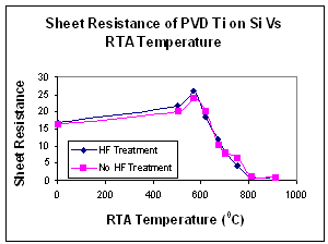
The pre deposition treatment appears to have no effect on silicide formation. In the 500 - 600°C temperature range the silicide produced would is high resistivity C49 phase of TiSi2. As the temperature increases the C49 phase gives way to the C54 phase characterised by the decrease in resistivity. This phase change is completed at approximately 800°C as has been well documented in other works. Nucleation of the C54 phase occurs at the triple points junction of the C49 phase.
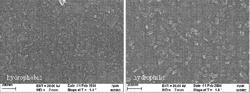
SEM analysis of the silicide layers showed the layer with no interface oxide exhibited a larger variation in grain size and structure compared to the silicide formed with an oxide interlayer.
Cobalt Silicide
Polycrystalline CoSi2 currently in use has the advantage over other silicides in that the low resistivity silicide phase is not inhibited by geometry and silicide formation is through the diffusion of cobalt rather than silicon. This prevents lateral growth and removes the possibility of short circuits. CoSi2 also enjoys greater thermal stability and uniformity over other silicides, crucial for the implantation and annealing steps in device fabrication.
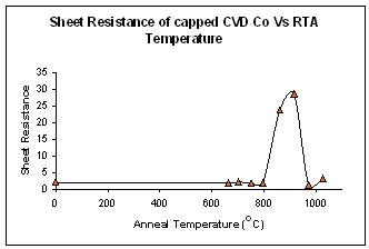
Cobalt silicide formation was investigated from cobalt deposited by CVD. The initial reaction between the substrate and the precursor produced a thin oxide layer prior to any cobalt deposition. The thin oxide layer prevents cobalt diffusion at lower temperatures as can be seen below. This allowed the possibility of producing an epitaxial CoSi2 layer though an oxide mediating epitaxy (OME) scheme.
A CVD cobalt layer was deposited on silicon at 450°C, after annealing it was found that no metal rich CoSi2 phase formed, at 800°C the high resistivity CoSi phase formed as the anneal temperature increased to 950°C CoSi2 formed. The high temperature required to form a silicide and the non existence of the Co2Si phase are attributed to the oxide at the interface.
The oxide thickness has been estimated using capacitance measurements to be 26Å, which would agree well with the findings of other groups.
Nickel Silicide
Self-aligned silicidation (silicidation) has become an essential process in complementary MOS technology to reduce the resistance of gate and source/drain regions. TiSi2 and CoSi2 have been used as silicide materials due to their low resistivity and high thermal stability. However as device dimensions shrink, TiSi2 encounters a problem in incomplete phase transformation to the low resistivity C54 phase at narrow line widths due to the lack of nucleation sites. CoSi2 is currently used due to its high thermal stability and the sheet resistance has no linewidth dependence. However CoSi2 is limited by high silicon consumption and junction leakage. The low resistivity of NiSi (14mWcm) makes it an attractive candidate for shallow junction leakage. In addition, it also offers the advantage of low silicon consumption (~1nm of Ni reacts with 1.84nm of silicon to form 2.22nm NiSi) and a single step low silicidation temperature.
The phase transformation of NiSi and high resistivity NiSi2 is known to be nucleation-controlled process, and occurs at temperatures of 750°C and above. Beside this transformation, agglomeration of the NiSi layer has been reported at annealing temperatures as low at 600°C.
Nickel Germanide
Nickel layers were deposited by PVD on germanium substrates and annealed at 350°C in an inert ambient
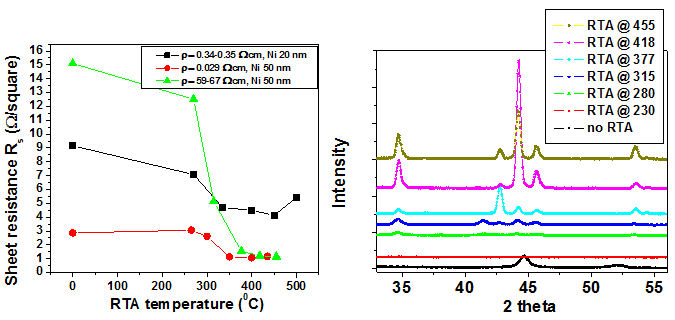
The figure above shows the variation of sheet resistance of nickel germanium compounds with RTA temperature. Also the resistivity of germanium substrate for each set of values is given.
From the figure it is clear that annealing at temperatures greater than 250OC yields the formation of NiGe. These samples were stripped of unreacted Ni and subjected to x-ray difraction analysis. XRD scans for nickel on germanium annealed at a range of temperatures confirmed the formation of NiGe at temperatures greater than 250OC.