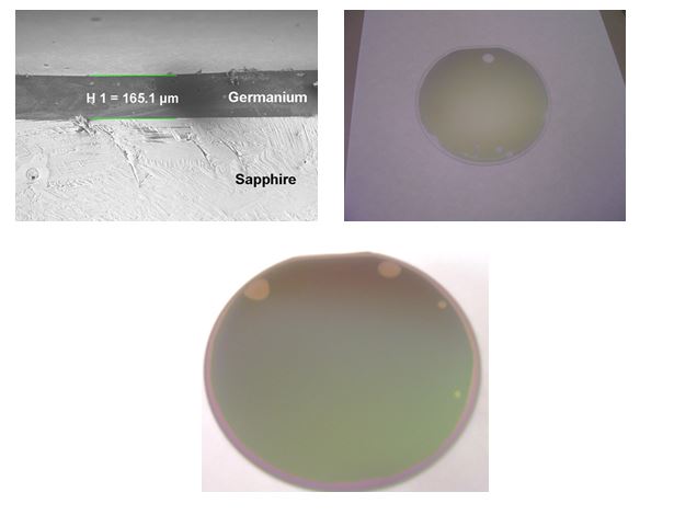
Germanium Bonding
Introduction
The rapid advances in the world of electronics over the past 50 years have been mainly due to silicon MOSFET technology. Through scaling of lateral and vertical dimensions of the MOSFET both circuit performance and complexity have been enhanced. Further progress through scaling alone is no longer possible and new materials have already been introduced for the gate dielectrics. The necessary gate capacitance requires a silicon dioxide layer so thin that tunnelling currents through it become excessively large. To overcome this problem silicon dioxide has been replaced with metal oxide dielectrics of higher permittivity. Thus the required capacitance can be achieved with dielectric layers thick enough to avoid tunnelling currents.
The replacement of silicon-dioxide by a deposited material of higher dielectric constant (high-k) breaks the uniqueness of the silicon dioxide-silicon interface. The confirmation that excellent electrical interface quality can be achieved reproducibly between a deposited high-k dielectric and silicon opens up the possibility for MOSFETs on other semiconductors. Germanium with an electron mobility twice that of silicon and a hole mobility four times that of silicon is a possible candidate for enhanced CMOS circuits. Germanium and gallium arsenide (GaAs) are lattice-matched offering the potential of germanium p-channel MOSFETs with n-channel MOSFETs on epitaxially grown GaAs layers to exploit both high mobility holes and high mobility electrons. Epitaxial GaAs on germanium offers the possibility of integrating optical and electronic circuits and of circuits employing mixed semiconductors.
Circular Geometry Ge self aligned MOS transistors
Germanium is not an abundant material. It is expensive, heavier and more fragile than silicon. It has a low energy bandgap and so has a higher junction leakage current. To overcome these disadvantages it is probable that germanium will be used in the form of a thin layer on an insulating substrate. Generally germanium-on-insulator (GeOI) refers to a thin germanium layer on an oxidised silicon substrate. This combination has advantages for processing on standard silicon production lines where the equipment has been optimised for handling silicon. However, there is considerable mismatch in temperature coefficient of expansions (TCEs) between silicon and germanium and silicon substrates can be lossy for very high performance rf and millimetre wave circuits. Silicon on sapphire technology (SOS) has been employed for many years, offering the same advantages that are obtained through SOI technology. Sapphire substrates are often preferred in rf and MMIC applications as they have excellent dielectric properties, which make them an excellent substrate for passive elements. Sapphire’s high resistivity also ensures low crosstalk through the substrate between noisy digital and sensitive analogue components. Sapphire will also provide reduced self-heating effects due to its higher thermal conductivity compared with that of silicon dioxide. Combining the two substrates, i.e., Germanium on Sapphire (GeOS), provides a unique platform for system on a chip (SOC) technology.
The GeOS platform provides good heat removal, low rf losses and low crosstalk for high frequency circuits, a lattice matched substrate for the growth of GaAs and matched coefficient of thermal expansion.
Germanium bonded to sapphire