
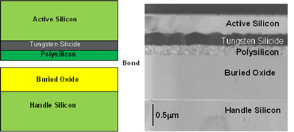
Silicon on Silicide on Insulator (SSOI) Substrates
The tunsgten silicide layer is deposited onto the active silicon substrate, this is then bonded to an oxidised silicon handle, as shown below. It has been shown that the high temperature bond anneal (typically 1050 2hrs) produces no asgglomeration in the silicide layer and that the quality of the active silcon is unaffected.
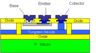
A number of applications have been demonstrated for such a substrate: a buried conduction layer to reduce collector resistance in the fabrication of SiGe HBTs, as shown in the diagram below.
In the fabrication of pin diodes to produce a phase shifter
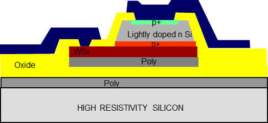
Mm-wave reflect-arrays offer flat profile and light weight, combined with many of the useful electrical characteristics of parabolic reflector antennas. By integrating diodes into the reflect-array structure the array can be made to perform the function of a spatial phase shifter, thereby permitting its use for beam steering applications.
In order to ensure high aperture efficiency, simulation has shown that the series loss resistance of these diodes must be less than 2W. To effectively minimise diode resistance it is necessary both to tightly control the thickness of the active silicon layer beneath the device junction, and also to provide a low resistance buried layer interconnect to this region. In addition, mm-wave transmission line losses must also be minimised.
Such a structure may be implemented using MBE, however this method has the disadvantage of high processing cost. As a realistic low-cost alternative, this work focussed on the fabrication of SSOI (Silicon on Silicide On Insulator) substrates produced on high resistivity silicon, using ion splitting and two stages of silicon wafer direct bonding.
This technology permitted the production of SSOI substrates with active silicon regions only 0.5µm thick utilising low resistivity tungsten silicide (WSix) as the buried layer interconnect material, thus providing a very suitable substrate for the fabrication of high frequency Schottky barrier diodes.
Buried reflector layer to produce back side confinement of a Quantum Cascade terahertz laser
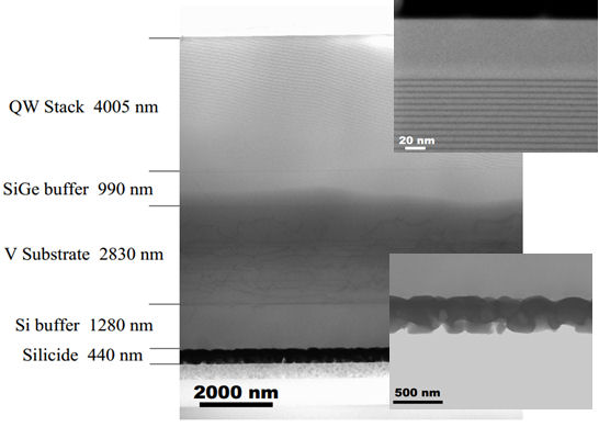
Micrograph shown a SSOI substrate with a virtual substrate grown by MBE on the surface. The quantum cascade laser structure is then grown in the virtual substrate and consists of alternating Si/SiGe layers typically 5nm thick.