Non-Standard Thermal Substrates
Non Standard Thermal Substrates
In most modern power semiconductor applications there is a need to carefully manage heat. This is particularly true of SOI devices as they exhibit self-heating effects. These arise because the device is thermally insulated from the bulk substrate by the buried oxide layer. This leads to a substantial elevation of temperature within the SOI device.
SOI has become an attractive technology for the fabrication of power devices. To remove the heat from a power MOSFET, a thermally conductive pathway from the MOSFET to ambient is needed, which usually includes some form of heat sink. Engineers at QAMEC have developed two approaches to enhance the removal of excess heat:
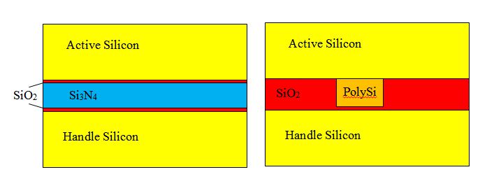
i) A non standard thermal substrate, which substitutes the buried oxide layer with a SiO2/Si3N4/SiO2 dielectric stack, was found to improving thermal performance significantly without compromising the electrical properties of the substrate.
ii) A thermal via is defined in the buried oxide prior to bonding and positioned such that it is under the hottest part of the device. The etched via is refilled with a thin oxide layer, CVD polysilicon, CMP is used to planarise the polysilicon to the oxide surface. This substrate is then bonded to the active silicon substrate.